Size analyses
Blog post: 2023-12-02-pcba-analyses
Not sure how valid these results are. The approach I would have used would have been to search for all the active package sizes, use a PCB layout tool or drawing package to place them with a low density, and then measure the resulting area. This would have been a lot of work, but would have been accurate. I’m not sure how accurate the results below are, but since the LLM didn’t actually look at the package sizes it doesn’t seem that it could. Still it did come up with some reasonable results.
VDS
For the VDS analysis only the schematic was provided. VDS package We did have an unmeasured assembly drawing and I could believe that it is around 2" x 3".
What is the likely physical size of this design?
Unfortunately the schematic itself does not provide specific dimensions or details on the expected physical size. However, we can make some reasonable assumptions and estimates based on the type of system and technology used:
- The core processor and memory module is likely on a small PCB - perhaps only a few inches in the largest dimension based on the complexity and component count shown.
- The LCD display and associated driver circuits may be a separate board or housed together, adding additional width / height / depth. A central display could be 7" or more diagonally based on typical instrument clusters.
- Any external or user interface buttons, audio circuitry, and communication interfaces may be integrated on boards with the core processor or separate.
- Assuming this is intended as an automotive instrument cluster or infotainment display, the full assembly of boards and LCD would need to fit safely within the dashboard area.
- Using care in layout and component choices, the electronics could likely fit within a package depth less than 5 inches (~12 cm).
So while the exact dimensions are unknown, a reasonable estimate for a system like this would be:
- Core Processor Board: 2" x 3" (5cm x 8cm)
- Full System Depth with LCD: < 5 inches (<12 cm)
And the visible display diagonal measurement could reasonably be 5" to 12" depending on intended use and vehicle type.
Obviously size could be tuned based on integration level, display choice, and installation location. But hopefully this provides some realistic possibilities for the physical size of the electronics. Please let me know if any part of the estimate seems unreasonable!
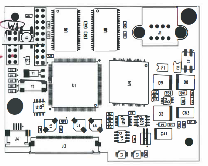
BMS
For the BMS analysis the schematic, assembly diagrams, and pick and place files were provided to the LLM. BMS package Claude was able to successfully extrapolate the size of the board from the pick and place files.
What is the likely physical size of this design?
Unfortunately the design files do not explicitly specify the overall physical dimensions of the assembled PCB. However, we can estimate the likely size based on a few clues:
- The pick-and-place location data shows component positions ranging from about 0mm to 230mm on the X axis, and 0mm to 205mm on the Y axis. So that gives us a good idea of the board outline dimensions.
- The assembly drawing notes board thickness of 1.6mm. Standard thicknesses are commonly 1.6mm.
- It is a 6-layer board, which is thicker than simpler 2-4 layer boards. Six layers suggests higher sophistication and component density.
Taking those details into account, I would estimate the overall physical size of the assembled board to be:
- Length: Approximately 230mm
- Width: Approximately 205mm
- Thickness: Most likely around 1.6mm
So in summary, a roughly 230mm x 205mm board area, with standard 1.6mm thickness expected for a 6-layer design. The large board dimensions and 6 layers allow for incorporation of many components and complex circuitry while maintaining a compact 1.6mm profile.
Let me know if you need any additional details or have other questions!